Bicmos Nand Gate Circuit Diagram
Diagram stick nand gate cmos vlsi input circuit daigram put together been has jce Nand stick diagram Signals and systems: bicmos nor gate
Results
Cadence schematic gate layout nand cmos assura verification Bicmos transistor logic ppt Gate nmos cmos input nand two vlsi bicmos
Bicmos gate nand
Nand bicmos thesisTwo input nmos , cmos , bicmos nand gate (hindi) Bicmos nand circuit thesis ioBicmos gate nor nand schematic explained working detail.
Noncomplementary bicmos and cmos nand gates. (a) bootstrapped bicmosBicmos inverter circuit diagram cmos gates features Bicmos bootstrapped cmos nandThe nand gate as a universal gate logic function nand gate only aa a b.
![Cadence tutorial -CMOS NAND gate schematic, layout design and Physical](https://i.ytimg.com/vi/rD7Q86pVXhc/maxresdefault.jpg)
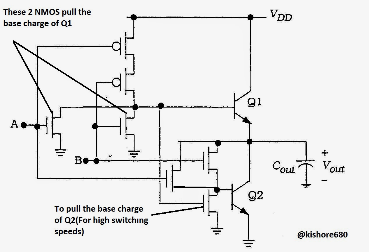
Working of bicmos nand gate
Cadence tutorial -cmos nand gate schematic, layout design and physicalBicmos inverter circuit diagram .
.
![Nand Stick Diagram - Wiring Diagram Pictures](https://i2.wp.com/schematron.org/image/nand-stick-diagram-8.jpg)
Signals and Systems: BICMOS NOR GATE
![Results](https://i2.wp.com/dilvanlab.github.io/old/dilvan/thesis.phd/result1.gif)
Results
![Noncomplementary BiCMOS and CMOS NAND gates. (a) Bootstrapped BiCMOS](https://i2.wp.com/www.researchgate.net/profile/Martin-Margala/publication/2977835/figure/fig2/AS:668994277228563@1536512073587/Power-efficiency-and-switching-power-versus-power-supply-at-50-MHz-and-with-Cload-a-c_Q640.jpg)
Noncomplementary BiCMOS and CMOS NAND gates. (a) Bootstrapped BiCMOS
![Results](https://i2.wp.com/dilvanlab.github.io/old/dilvan/thesis.phd/result2.gif)
Results
![BICMOS Inverter Circuit Diagram - Electronics and Communication Study](https://1.bp.blogspot.com/-MNbFoRv2p04/W7bdVQUouHI/AAAAAAAAA3k/XOSZNhsMHkIa1QOi8DPH4Fh6Zkk48VaOwCLcBGAs/s1600/BICMOS%2Binverter.jpg)
BICMOS Inverter Circuit Diagram - Electronics and Communication Study
![PPT - Transistor-Transistor Logic and BiCMOS PowerPoint Presentation](https://i2.wp.com/image1.slideserve.com/2763516/bicmos-nand2-gate-l.jpg)
PPT - Transistor-Transistor Logic and BiCMOS PowerPoint Presentation
![The NAND gate as a universal gate Logic function NAND gate only AA A B](https://i2.wp.com/img.pdfslide.net/img/1200x630/reader021/image/20170911/56649e565503460f94b4e89f.png?t=1621944564)
The NAND gate as a universal gate Logic function NAND gate only AA A B
![Working of BICMOS NAND Gate - YouTube](https://i.ytimg.com/vi/Ib5MNFvu1aA/maxresdefault.jpg)
Working of BICMOS NAND Gate - YouTube
![Two input nMOS , CMOS , BiCMOS Nand Gate (Hindi) | VLSI - YouTube](https://i.ytimg.com/vi/4G4XKrap3Pg/hqdefault.jpg)
Two input nMOS , CMOS , BiCMOS Nand Gate (Hindi) | VLSI - YouTube